Détection des nanoparticules chargées par un capteur à base de silicium sur isolant avec contacts métalliques : prévue de concept de deux méthodes de lecture originales, les fluctuations du courant et le potentiel hors-équilibre.
Publié le : 20 octobre 2020
Silicon on insulator sensor with metal deposited contacts for detection of charged nanoparticles:
proof of concept of two original electrical methods: fluctuation-enhanced sensing and out-ofequilibrium
body potential
FMNT laboratories involved/Advisors:
IMEP-LAHC: C. Theodorou, christoforos.theodorou@grenoble-inp.fr; I. Ionica, Irina.Ionica@grenoble-inp.fr
LMGP: Marianne Weidenhaupt, marianne.weidenhaupt@grenoble-inp.fr
Context/objectives:
In the wide family of bio-chemical sensors, the ISFETs (Ion Sensing Field Effect Transistors) occupy a place of honor thanks to their multiple advantages, e.g. in terms of miniaturization, sensitivity, cointegration with reading circuitry etc¹. The working principle of such a device is based on the shift of the threshold voltage of a transistor, due to the intentional addition of charges-to-be-detected in the proximity of its channel. The resulting conductivity/ drain-current modulation is then measured in (quasi)-static conditions, in which externally applied voltages are slow enough and the device is assumed at equilibrium at every measurement point.
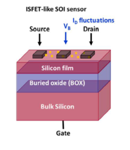
In this context, the objective of the internship is to prove the feasibility of detection based on two original dynamic methods, exploited in a simple FET-like sensor made of silicon-on-insulator:
- Monitoring the evolution of out-of-equilibrium potential VB of the top semiconductor in presence of the molecules to-be-detected. The interest of measuring VB instead of drain current/conductance resides in the fact that the potential signature is very strong in the region were the drain current level is very small ²; this simplifies the measurement and can reduce the power consumption of the sensor.
- Monitoring the drain current fluctuations in time by noise measurements. This principle is based on the effects of dynamic interaction between surface traps and electrons of deposited molecules, leading to a unique characteristic noise spectrum for each sensing target³. An increased sensitivity, as well as a better selectivity, can be expected with this approach.

During the internship, validation of the proposed methods will be performed thanks to simple “model” charges such as carboxylate-functionalized polystyrene latex beads deposited on the Si film surface. The interest in starting with such particles resides in the simplicity of the deposition from colloidal solutions, without any need of surface functionalization. The amount of charges can also be simply tuned by derail dilutions of the beads or mixtures of charges and uncharged beads.Requested competences:The internship is dealing with an interdisciplinary topic, covering a wide panel of know-hows, from the semiconductor device physics at equilibrium, in out-of-equilibrium/dynamic conditions, to electrical characterization and modeling (C. Theodorou, M. Bawedin, I. Ionica from IMEP-LAHC), to the chemistry of the particles and, later-on, bio-sensing (M. Weidenhaupt from LMGP). The candidate must have a very good background in semiconductor physics, characterization of semiconductor devices. Knowledge of concepts in bio-chemical sensing will be a plus.The candidate is expected to enjoy experimental work and development of adapted protocols. Scientific curiosity and motivation are mandatory qualities in order to take full advantage of the multidisciplinary scientific environment of this internship and to gain expertise for his/her future career.To apply send your CV to: christoforos.theodorou@grenoble-inp.fr and Irina.Ionica@grenoble-inp.fr
__________________________________________________________________________________________________________
1 Bergveld, P. Sensors and Actuators B: Chemical 2003, 88, (1), p.1; Moser, N. et.al., IEEE Sensors Journal 2016, 16, (17), p. 6496.
2 Benea, L. et.al., Solid-State Electronics 2018, 143, p. 69.
3 Kish, L. B. et.al.,IEEE Trans. on Nanotechnology 2011, 10, (6), p. 1238; Rumyantsev, S. et.al., IEEE Sensors Journal 2013, 13, (8), p. 2818


 Contactez-nous
 Plan d’accès


